One of the coolest, tucked-away features in the SAMD21 is the fractional digital phase locked loop (FDPLL). I still only have a vague idea of how phase locked loops (PLLs) work, but nonetheless, we can use the SAMD21’s PLL to create a 96 MHz clock.
The bad news is that, to the best of my knowledge, you cannot use this clock signal as the main clock source for the SAMD21 (essentially overclocking it). However, we can use it to power some other peripherals, like the generic clocks, timers, and pulse width modulation (PWM) signals.
If you are not familiar with how the clocks on the SAMD21 work, I recommend reading my previous post. You will also need to refer to the SAMD21 datasheet.
Let’s take a look at how you use the FDPLL on the SAMD21.
Step 1: Select a Clock Source
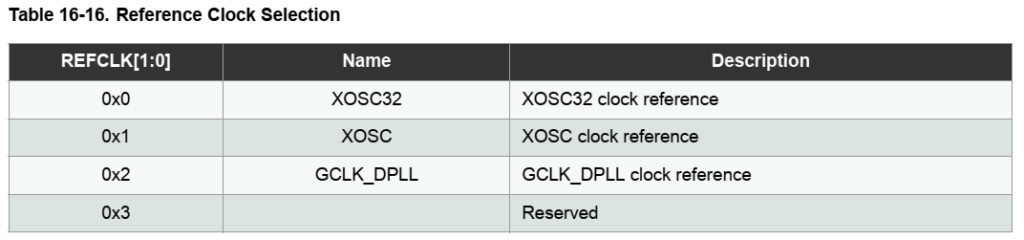
The FDPLL isn’t a standalone clock. You’ll need to select a source to feed the PLL, and the source clock needs to be in the 32 kHz to 2 MHz range. According to section 16.8.19 (page 208) of the datasheet, there are only 3 acceptable clock sources for the FDPLL: XOSC32, XOSC, and a specific GCLK (known as GCLK_DPLL). You can set the clock source for the PLL in the DPLLCTRLB register.
Step 2: Configure FDPLL
Next, you will need to set the frequency multiplier in DPLLRATIO register. There are two numbers you must configure: the ratio (LDR bits) and the ratio fractional part (LDRFRAC bits). The equation below (from section 16.6.8.3, page 158) shows how to calculate the output frequency of the FDPLL. fclk_fdpll96m is the output frequency and fclk_fdpll96m_ref is the reference clock (the input clock source).
![]()
So, if we want to turn a 1 MHz clock source into a 96 MHz output, we would set LDR to 95 and LDRFRAC to 0.
Step 3: Turn It On
By default, the FDPLL is disabled on reset. To enable it, we just write a 1 to the ENABLE bit in the DPLLCTRLA register.
Step 4: Use It!
The FDPLL can be used as a clock source for any of the generic clocks found in the generic clock controller. This includes the USB clock, watchdog timer, clock channels, SERCOMs, etc. Section 14.8.3 (page 107) has a table (too big to copy here) that gives you an idea of the available GCLKs. If you use one of the GCLK channels, you can use it to clock a peripheral, like PWM!
Example: A More Complicated 1 MHz Signal
In my last post, I showed you how to create a 1 MHz signal using GCLK4, TCC2, and a PWM peripheral. Let’s do the same thing, but in a much more roundabout way!
We’ll feed GCLK4 from the main 48 MHz clock, divide the clock by 48, feed that signal to GCLK_DPLL, which is then sent to the FDPLL. The DPLL will create a 96 MHz clock signal, which we’ll send to GCLK5 to be used as the basis for TCC2 and our PWM signal. This diagram should offer a much better explanation of what’s going on:
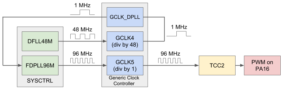
Because our PWM clock is running twice as fast as in the previous example, we’ll need to adjust the TOP to be twice as high. We’ll use 95 instead of 47 to achieve our 1 MHz signal.
Here is the Arduino code to accomplish this:
// I have no idea why these definitions were left out of the Arduino headers
#define GCLK_GENCTRL_SRC_DPLL96M_Val 0x8ul  // (GCLK_GENCTRL) DPLL96M output
#define GCLK_GENCTRL_SRC_DPLL96M (GCLK_GENCTRL_SRC_DPLL96M_Val << \
                                  GCLK_GENCTRL_SRC_Pos)

// Number to count to with PWM (TOP value). Frequency can be calculated by
// freq = GCLK4_freq / (TCC2_prescaler * (1 + TOP_value))
// With TOP of 95, we get a 1 MHz square wave in this example.
// TCC2 is 16 bits
uint16_t period = 96 - 1;

void setup() {

  // Flash wait states NVMCTRL->CTRLB.bit.RWS set to 1 by Arduino framework

  // Configure generic clock generator 4
  GCLK->GENCTRL.reg = GCLK_GENCTRL_IDC |          // Improve duty cycle
                      GCLK_GENCTRL_GENEN |        // Enable generic clock gen
                      GCLK_GENCTRL_SRC_DFLL48M |  // Select 48MHz as source
                      GCLK_GENCTRL_ID(4);         // Apply to GCLK4
  while (GCLK->STATUS.bit.SYNCBUSY);              // Wait for synchronization

  // Set clock divider of 48 to generic clock generator 4 (1 MHz)
  GCLK->GENDIV.reg = GCLK_GENDIV_DIV(48) |        // Divide 48 MHz by 48
                     GCLK_GENDIV_ID(4);           // Apply to GCLK4 4
  while (GCLK->STATUS.bit.SYNCBUSY);              // Wait for synchronization

  // Enable GCLK4 and connect it to GCLK_DPLL
  GCLK->CLKCTRL.reg = GCLK_CLKCTRL_CLKEN |        // Enable generic clock
                      GCLK_CLKCTRL_GEN_GCLK4 |    // Select GCLK4
                      GCLK_CLKCTRL_ID(1);         // Feed GCLK4 to GCLK_DPLL
  while (GCLK->STATUS.bit.SYNCBUSY);              // Wait for synchronization

  // Set DPLL ratio to 1 MHz * (95 + 1) = 96 MHz
  SYSCTRL->DPLLRATIO.reg = SYSCTRL_DPLLRATIO_LDRFRAC(0) | // Ratio fractional
                           SYSCTRL_DPLLRATIO_LDR(95);     // Ratio

  // Configure DPLL to disregard phase lock and select GCLK as source
  SYSCTRL->DPLLCTRLB.reg = SYSCTRL_DPLLCTRLB_LBYPASS |    // Bypass lock
                           SYSCTRL_DPLLCTRLB_WUF |        // Wake up fast
    SYSCTRL_DPLLCTRLB_REFCLK(SYSCTRL_DPLLCTRLB_REFCLK_GCLK_Val); // Select GCLK

  // Enable DPLL
  SYSCTRL->DPLLCTRLA.reg |= SYSCTRL_DPLLCTRLA_ENABLE;

  // Configure generic clock generator 5
  GCLK->GENCTRL.reg = GCLK_GENCTRL_IDC |          // Improve duty cycle
                      GCLK_GENCTRL_GENEN |        // Enable generic clock gen
                      GCLK_GENCTRL_SRC_DPLL96M |  // Select DPLL as source
                      GCLK_GENCTRL_ID(5);         // Apply to GCLK5
  while (GCLK->STATUS.bit.SYNCBUSY);              // Wait for synchronization

  // Set clock divider of 1 to generic clock generator 5 (96 MHz)
  GCLK->GENDIV.reg = GCLK_GENDIV_DIV(1) |        // Divide 96 MHz by 1
                     GCLK_GENDIV_ID(5);           // Apply to GCLK5
  while (GCLK->STATUS.bit.SYNCBUSY);              // Wait for synchronization

  // Enable GCLK5 and connect it to TCC2 and TC3
  GCLK->CLKCTRL.reg = GCLK_CLKCTRL_CLKEN |        // Enable generic clock
                      GCLK_CLKCTRL_GEN_GCLK5 |    // Select GCLK5
                      GCLK_CLKCTRL_ID_TCC2_TC3;   // Feed GCLK5 to TCC2/TC3
  while (GCLK->STATUS.bit.SYNCBUSY);              // Wait for synchronization

  // Divide counter by 1 giving 96 MHz (10.42 ns) on each TCC2 tick
  TCC2->CTRLA.reg |= TCC_CTRLA_PRESCALER(TCC_CTRLA_PRESCALER_DIV1_Val);

  // Use "Normal PWM" (single-slope PWM): count up to PER, match on CC[n]
  TCC2->WAVE.reg = TCC_WAVE_WAVEGEN_NPWM;         // Select NPWM as waveform
  while (TCC2->SYNCBUSY.bit.WAVE);                // Wait for synchronization

  // Set the period (the number to count to (TOP) before resetting timer)
  TCC2->PER.reg = period;
  while (TCC2->SYNCBUSY.bit.PER);

  // Set PWM signal to output 50% duty cycle
  // n for CC[n] is determined by n = x % 4 where x is from WO[x]
  TCC2->CC[0].reg = period / 2;
  while (TCC2->SYNCBUSY.bit.CC0);

  // Configure PA16 (D11 on Arduino Zero) to be output
  PORT->Group[PORTA].DIRSET.reg = PORT_PA16;      // Set pin as output
  PORT->Group[PORTA].OUTCLR.reg = PORT_PA16;      // Set pin to low

  // Enable the port multiplexer for PA16
  PORT->Group[PORTA].PINCFG[16].reg |= PORT_PINCFG_PMUXEN;

  // Connect TCC2 timer to PA16. Function E is TCC2/WO[0] for PA16.
  // n for PMUX[n] is given by floor(pin_num / 2)
  // Odd pin num (2*n + 1): use PMUXO
  // Even pin num (2*n): use PMUXE
  PORT->Group[PORTA].PMUX[8].reg = PORT_PMUX_PMUXE_E;

  // Enable output (start PWM)
  TCC2->CTRLA.reg |= TCC_CTRLA_ENABLE;
  while (TCC2->SYNCBUSY.bit.ENABLE);              // Wait for synchronization
}

void loop() {
  // Do nothing
}
This is certainly a crazy, circuitous route to take for a 1 MHz signal, but it offers much greater control of the PWM frequency. If your application needs this kind of control (e.g. motor controls), firing up the PLL could be incredibly helpful.
In case you’re wondering where I’m going with this project: let’s just say that this fine control of clock speeds lets us create something like a digitally controlled oscillator (DCO).
Thanks for this! I have stolen, I mean used, some of your code in a PWM library for Arduinos: https://github.com/ocrdu/Arduino_SAMD21_turbo_PWM
Awesome! Glad it helped 🙂