Introduction
Free, online development and CAD tools are becoming more popular and powerful, and PCB layout tools are no exception. In this, we are going to look at how to create a simple schematic in EasyEDA, turn it into a PCB, and send out the design files to a PCB house for fabrication.
We will do this in several parts–starting with part creation, then schematic capture, and PCB layout before sending out files for board fabrication. By the end, we’ll have made a simple linear regulator that supplies 5V and up to 1A to a breadboard and accepts a barrel jack from a wall adapter to provide power.
Signing Up
Head to easyeda.com, and click Login at the top of the page. While you can start without an account, being able to save projects to your account is quite useful.
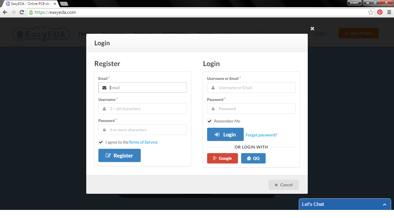
Fill out your information and click Register.
New Project
When you have logged in, click New Project at the top of the screen, and you will be presented with the main project screen. Click on Create a new project under the Start tab and give your project an appropriate name. In this tutorial, we will be creating a DC/DC converter using a simple linear regulator, so I’ll name mine “5V Power Supply.”
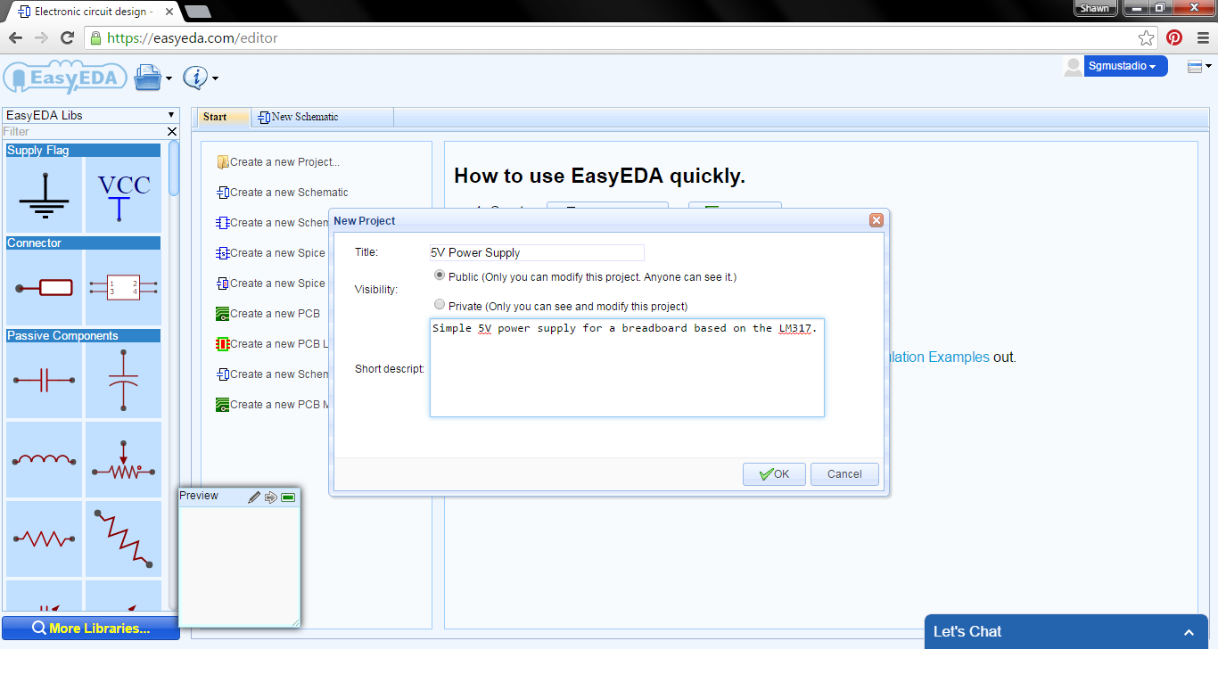
Feel free to keep it private (or not if you want to share it) and add a short description. Click OK.
Package Creation
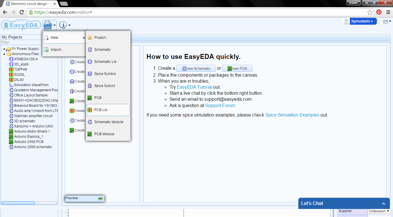
Luckily, EasyEDA has a wide range of parts for us to use. We will base our design around the LM317 for DC/DC conversion, and we’ll put a barrel jack on the board so we can plug it into a wall outlet. Unfortunately, there is no barrel jack part or package in EasyEDA, so we’ll need to make one. We’ll base our design on the PJ-002AH-SMT-TR from Digi-Key. The first order of business is to create the package (footprint) for the part.
Click on the File icon on the top of the window, and select New. Click on PCB Lib.
You’ll notice that the units are in imperial, so we’ll change our canvas units. In the right-side pane, under Canvas Attributes, select mm from Units.
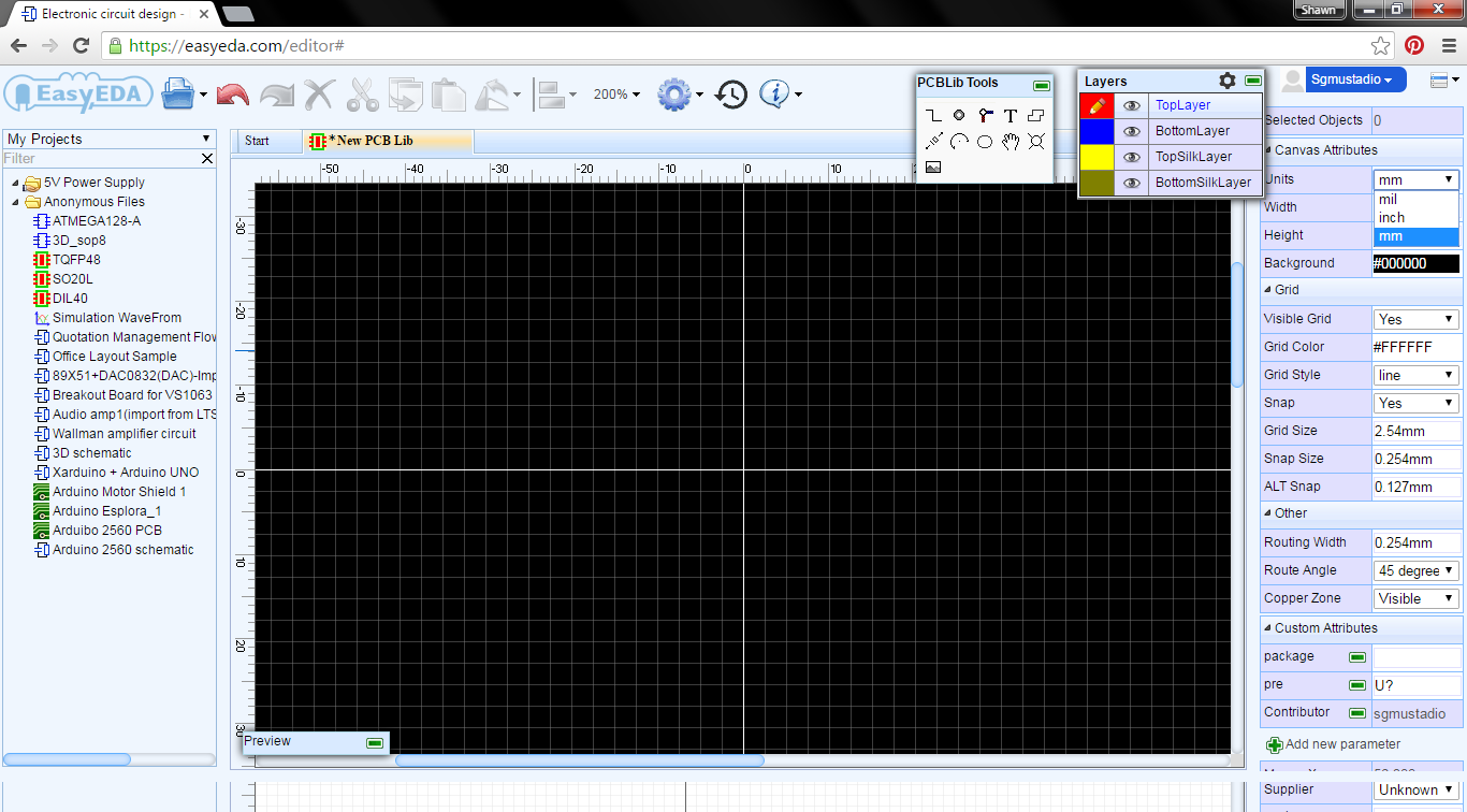
We will be looking at the barrel jack’s datasheet for the dimensions we need. Click on Pad in the PCBLib Tools box (circled in red in the image).
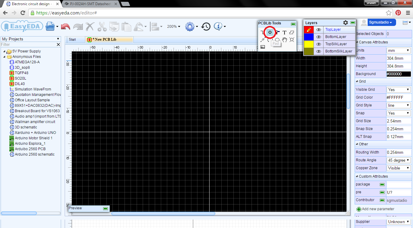
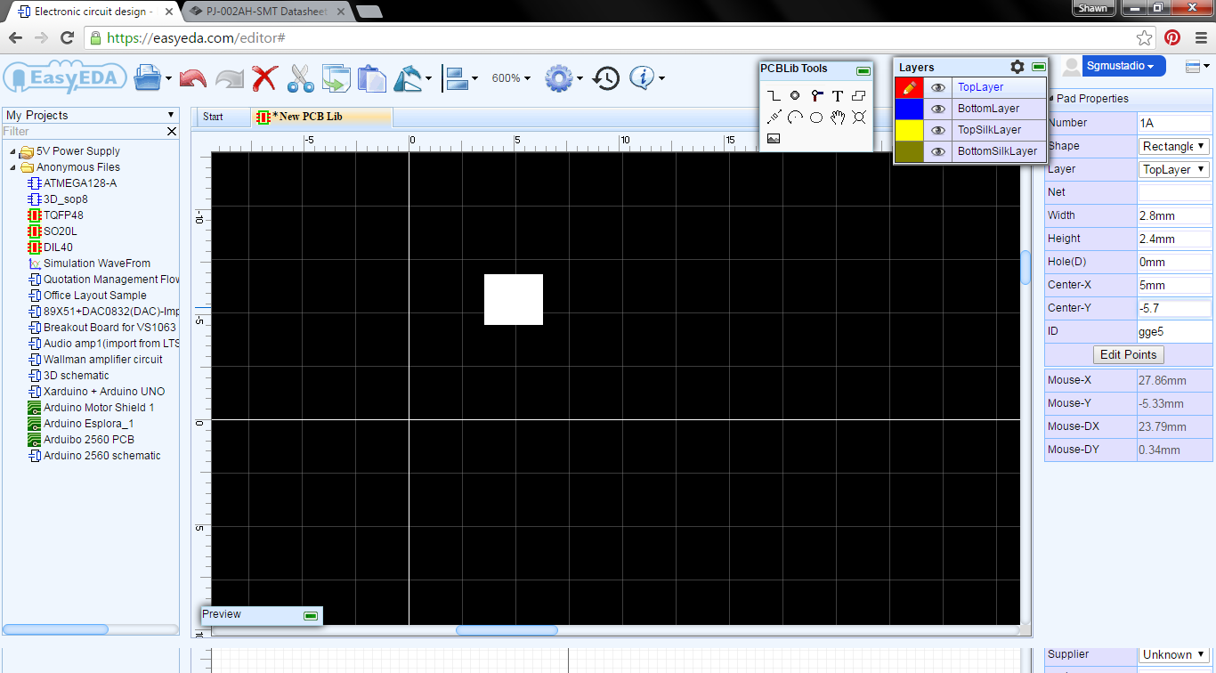
Click somewhere in the layout to drop the pad. Hit esc to stop placing pads. Click on the pad to edit its attributes. Change the following:
- Name: 1A
- Shape: Rectangle
- Layer: TopLayer (so it becomes a surface mount pad)
- Width: 2.8 (mm)
- Height: 2.4
- Hole: 0
- Center-X: 5
- Center-Y: -5.7
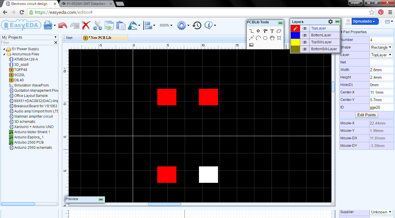
Place 3 more pads with the following attributes:
Pad 1B:
- Name: 1B
- Shape: Rectangle
- Layer: TopLayer (so it becomes a surface mount pad)
- Width: 2.8 (mm)
- Height: 2.4
- Hole: 0
- Center-X: 11.1
- Center-Y: -5.7
Pad 2:
- Name: 2
- Shape: Rectangle
- Layer: TopLayer (so it becomes a surface mount pad)
- Width: 2.8 (mm)
- Height: 2.4
- Hole: 0
- Center-X: 11.1
- Center-Y: 5.7
Pad 3:
- Name: 3
- Shape: Rectangle
- Layer: TopLayer (so it becomes a surface mount pad)
- Width: 2.8 (mm)
- Height: 2.4
- Hole: 0
- Center-X: 5
- Center-Y: 5.7
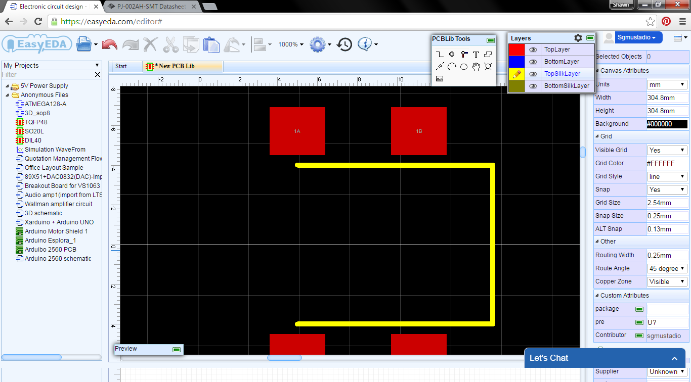
In the layers box, click on the yellow box next to TopSilkLayer to edit the top silk screen. In the PCBLib Tools box, select Track.
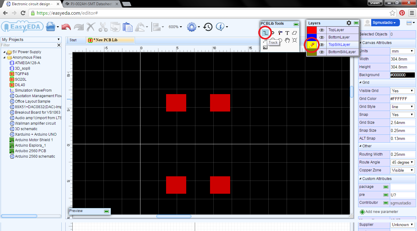
Draw three separate, unconnected lines. We want to leave the front open so we can have some of the component hanging off the PCB. Right-click to end placement of the lines.
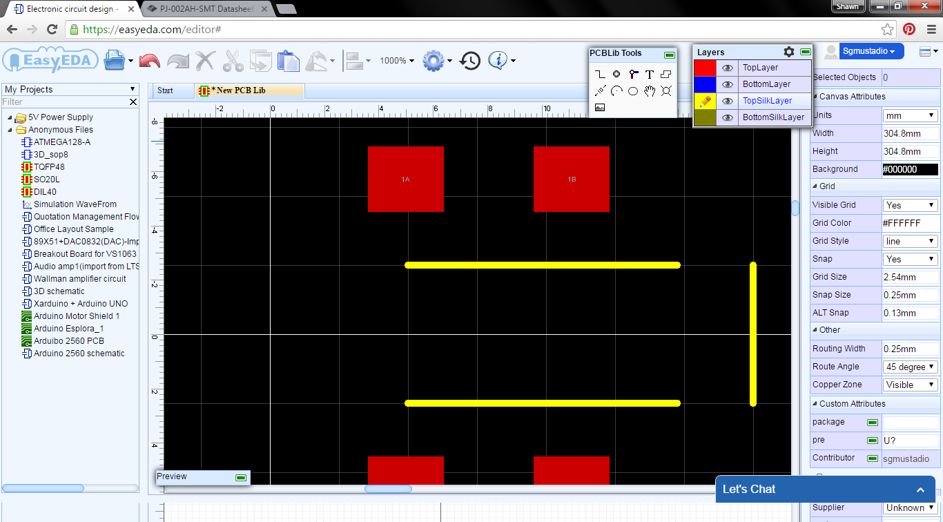
Adjust the lines’ properties so that they make an open rectangle. Click on each one and change their attributes:
Line 1:
- Start-X: 5mm
- Start-Y: -4mm
- End-X: 14.8mm
- End-Y: -4mm
Line 2:
- Start-X: 14.8mm
- Start-Y: -4mm
- End-X: 14.8mm
- End-Y: 4mm
Line 3:
- Start-X: 5mm
- Start-Y: 4mm
- End-X: 14.8mm
- End-Y: 4mm
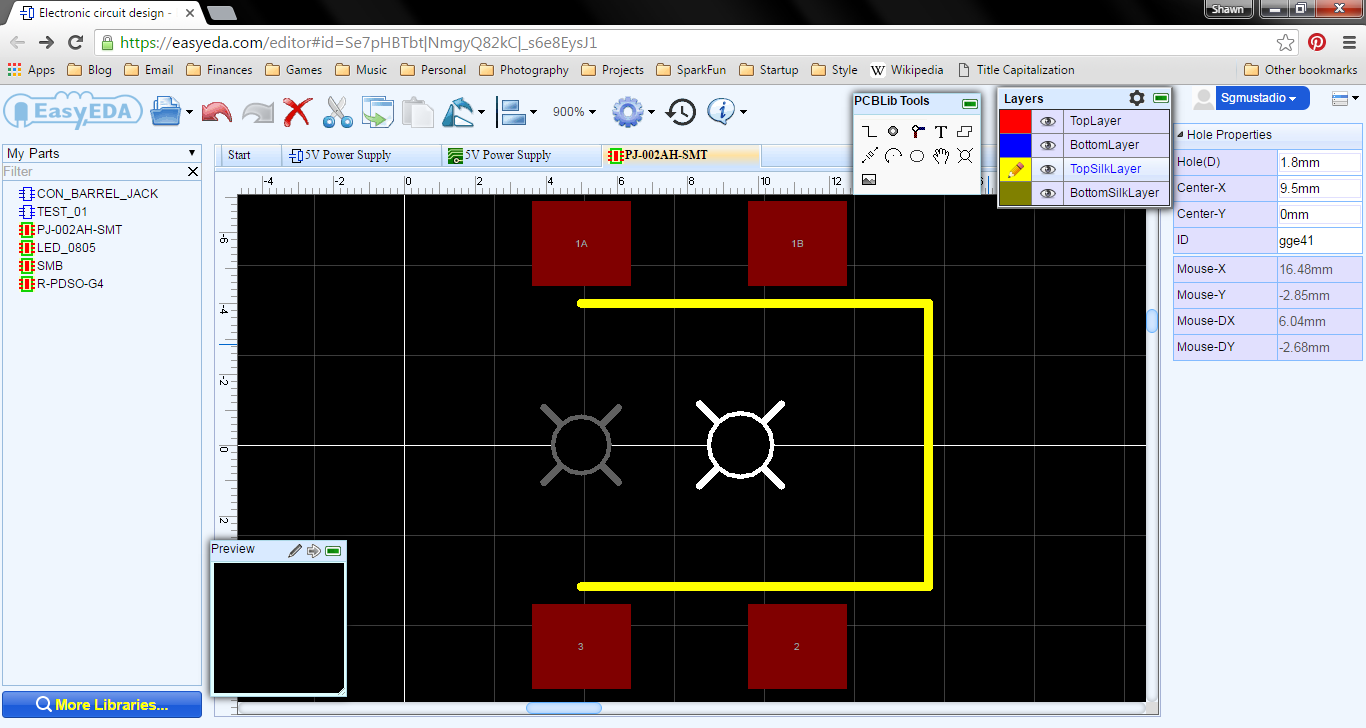
Finally, we need to add a couple of holes for the part’s posts. Click on the Hole icon in the PCBLib Tools box.
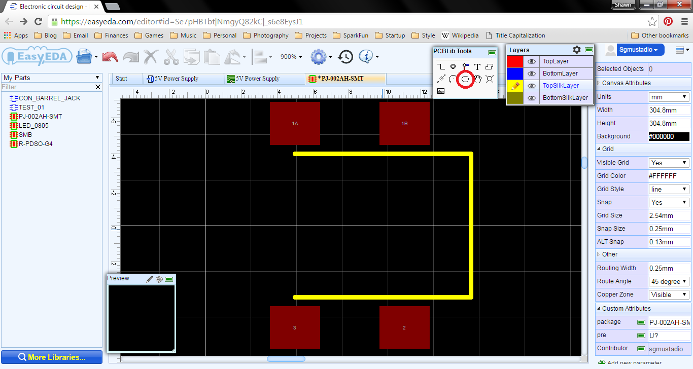
Place two holes, and change their properties:
Hole 1:
- Hole(D): 1.6mm
- Center-X: 5mm
- Center-Y: 0mm
Hole 2:
- Hole(D): 1.8mm
- Center-X: 9.5mm
- Center-Y: 0mm
Click on the File icon, and select Save As. Give it a unique name, like PJ-002AH-SMT (manufacturer’s part name) and a short description, if you desire.
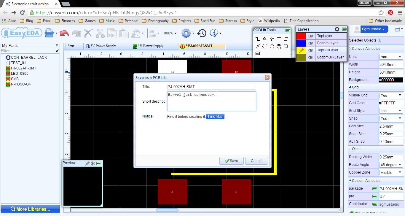
Click Save. That’s it for package creation!
Schematic Part Creation
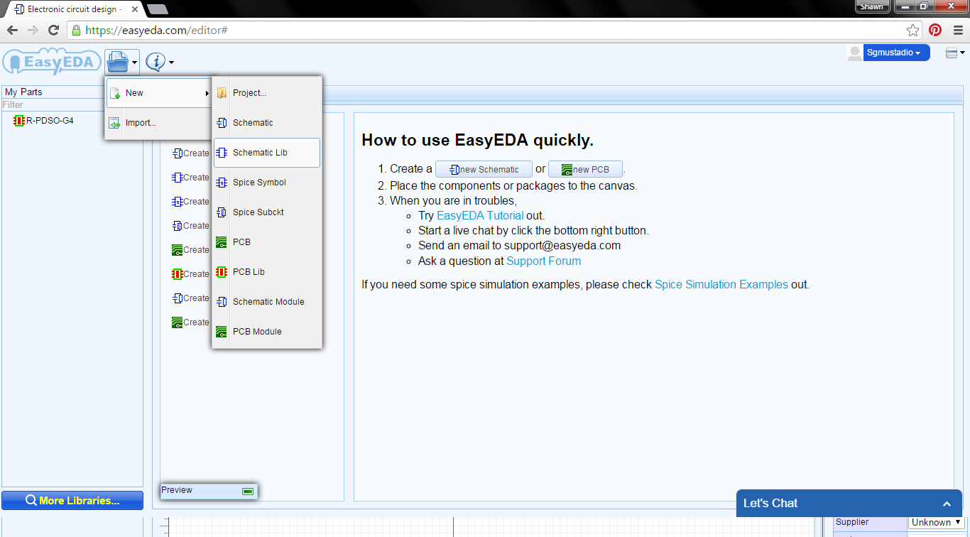
With the footprint complete, we need to create a schematic part. Click on the File icon, and select New. click on Schematic Lib.
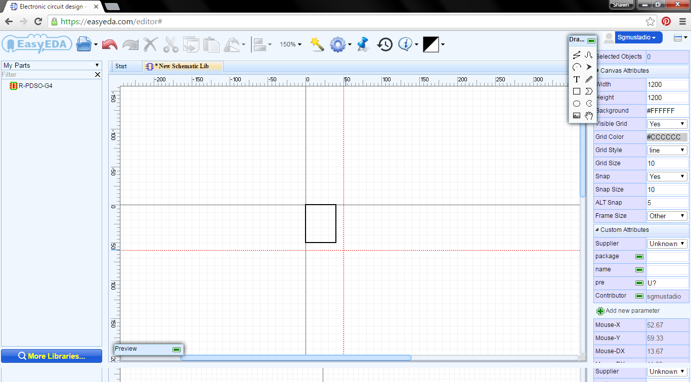
From the Drawing toolbox, select Rectangle.

Click once at the origin (intersection of the two dark lines), move the mouse down and to the right, and click again to create a rectangle. This will be the body of the schematic symbol for our part.
Click on the Pin icon, and click just outside the rectangle to create a pin. Move down a grid square and click. Repeat 2 more times for a total of 4 pins. Note that the pin’s connector (the circle at the end of the pin) should be facing away from the part body.
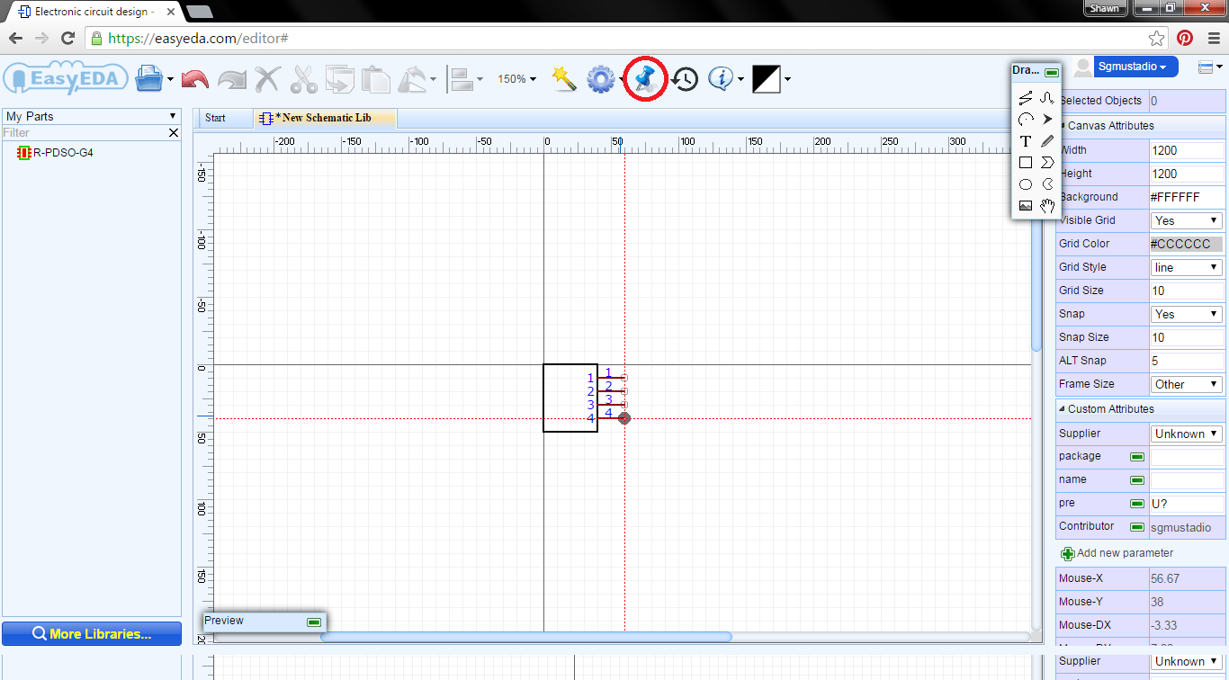
Press esc to stop placing pins. Click on the first pin to highlight it. In the attributes panel on the right, change:
- Name: TIP
- Number: 1A
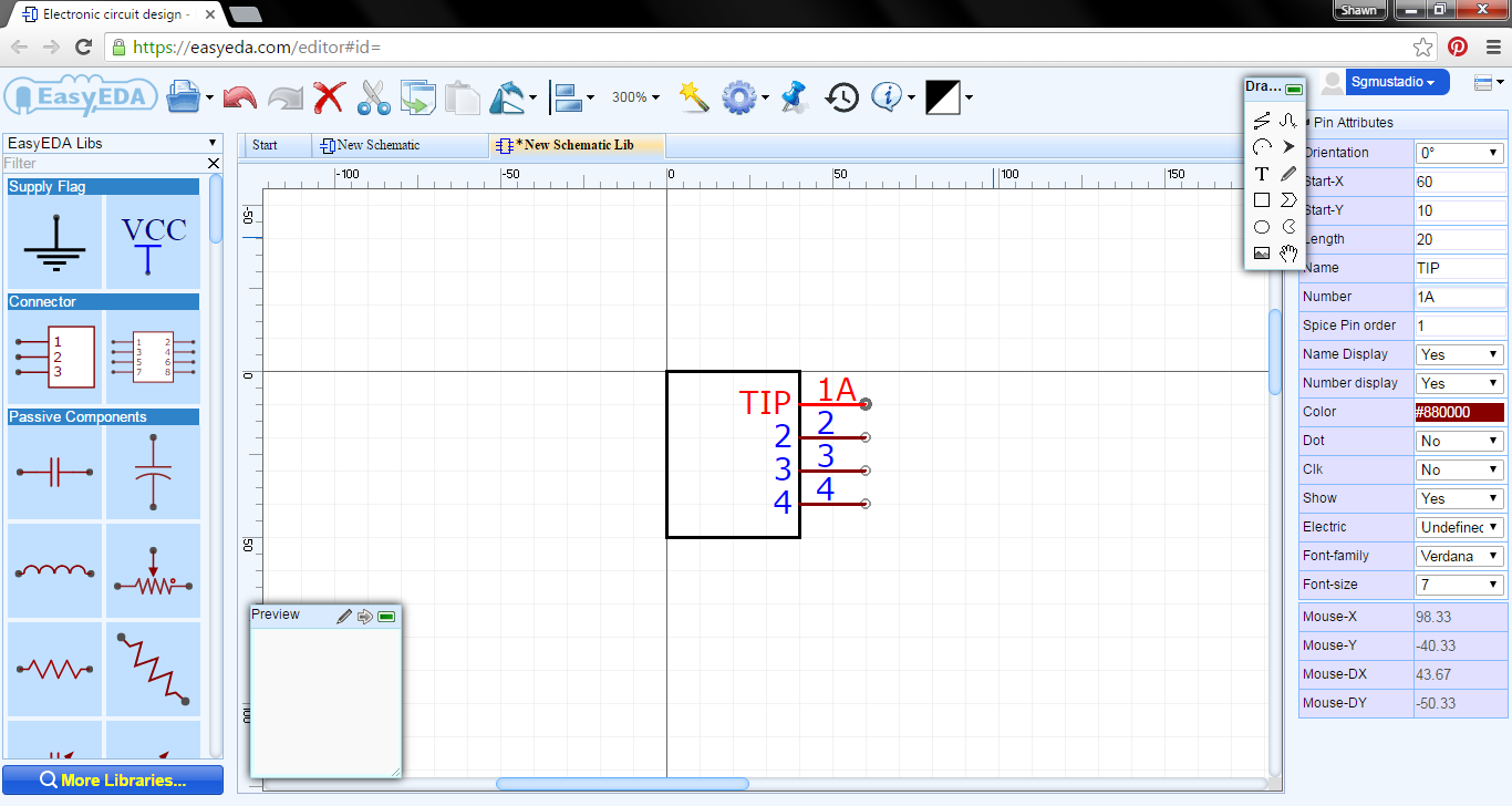
Do the same for the rest of the pins.
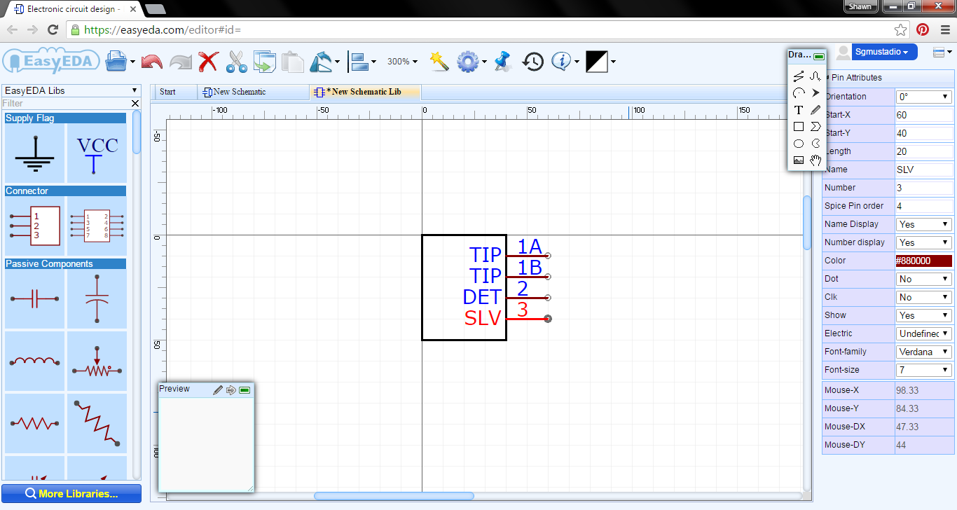
Pin 2:
- Name: TIP
- Number: 1B
Pin 3:
- Name: DET
- Number: 2
Pin 4:
- Name: SLV
- Number: 3
Click outside the part so that you see Canvas Attributes and Custom Attributes in the right-side pane. In Custom Attributes, change pre to J?. Click on the package entry box (below the pre box) to bring up the package selector box.
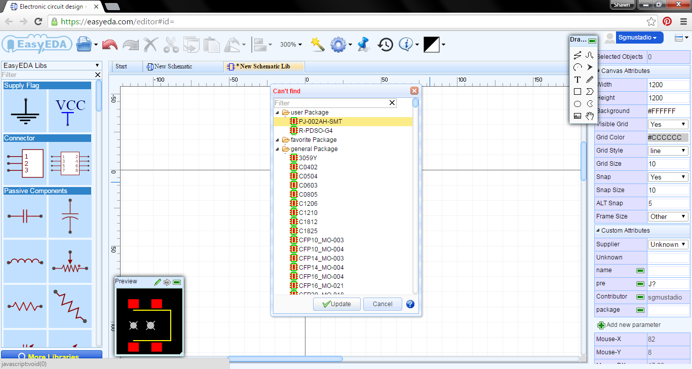
Under User Package, find the part we just made (PJ-002AH-SMT), select it, and click Update. Close the package selector box.
Click the File icon, select Save As, and fill out the part information. I named my part “CON_BARREL_JACK” and gave it a short description.
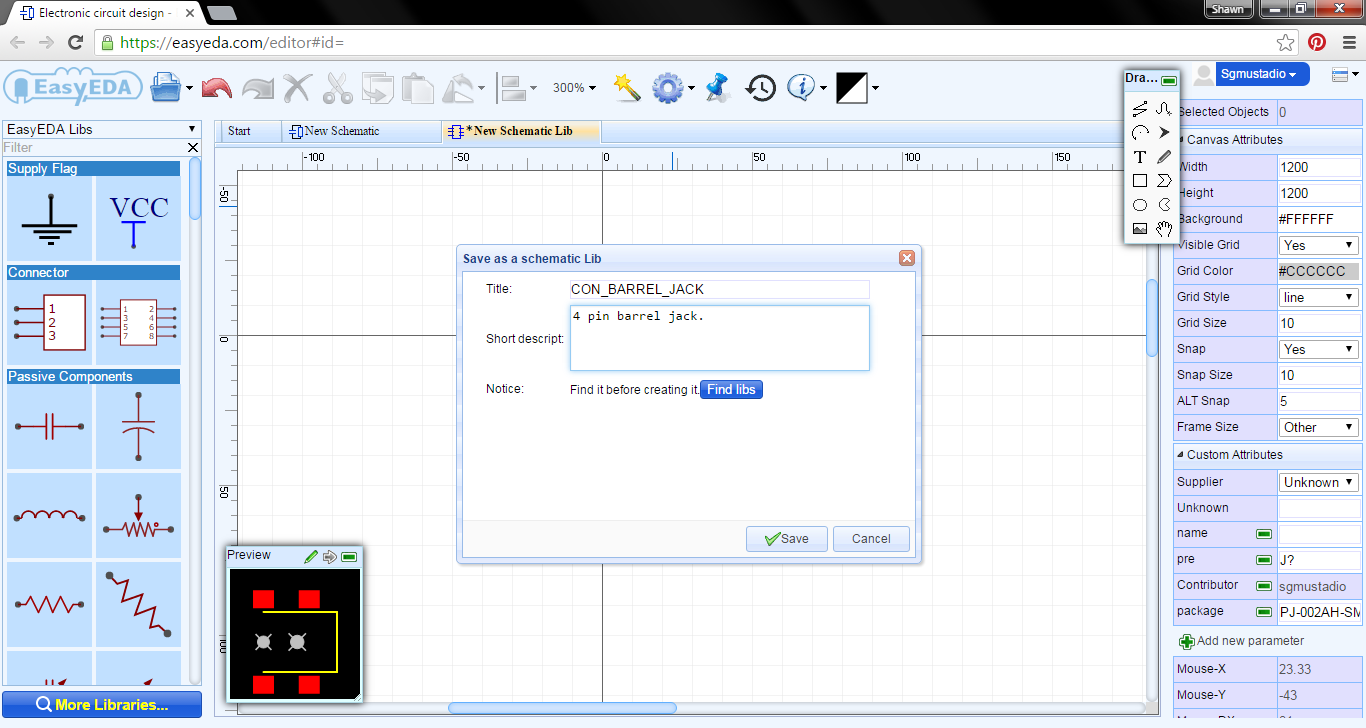
Click Save. We’re done with part creation, and tomorrow we’ll move on to schematic capture.
[…] Link to the Very Nice Tutorial I followed: PART1, PART2, PART3 […]
Hey there just wanted to give you a quick heads up. The words in your content seem to
be running off the screen in Opera. I’m not sure if this is a formatting issue or something to do with web browser compatibility but I figured I’d post to let you
know. The design look great though! Hope you get the
issue resolved soon. Thanks
I don’t have a Mac to check it, but I’ll look into it. Thanks!
This is now out of date as PCB Lib and Schematic Lib no longer exist in the package.