Arduino has a habit of making pulse width modulation (PWM) pins with a set frequency (or limited frequency options). For the average user, this is not a bad thing, considering it hides all the ugliness (or beauty, depending on your perspective) of manually setting registers.
For those of us that want to dig deeper into the SAMD21, there are a few options. Almost all modern implementations of the ARM Cortex architectures can use the Cortex Microcontroller Software Interface Standard (CMSIS). This is a set of firmware libraries that provide an interface to the registers along with some other functions. Ideally, you should be able to use CMSIS regardless of the manufacturer of the chip (e.g. Microchip, STMicroelectronics, TI).
Some vendors have decided to include their own abstraction layer on top of CMSIS to help people configure and use their parts. In some cases, this can make setting up registers easy (especially if there is a slick GUI program that generates code for you, like STMicro’s STM32CubeMX). Microchip’s abstraction layer is known as the Advanced Software Framework (ASF).
Many professional developers swear by the vendor-provided abstraction layer (e.g. ASF). If you’re like me, you want to know what’s going on at the register level. Not that there is anything wrong with ASF, I just like to learn about the low-level stuff.
Here’s the problem: when it comes to manually configuring registers for 32-bit ARM microcontrollers, it’s vastly more difficult than it is for most other 8- or 16-bit architectures.
I’ve spent the last few days digging through the SAMD21 datasheet and online examples to get some insight into using CMSIS. On the surface, it’s not too bad: you just need to set some values in some registers to get a pin to output a square wave. In reality, it requires a good amount of code to perform this simple action.
Please note that I am just beginning to understand how the SAMD21 works, and this article is simply a chronicle of my learning journey. If you think I missed something or got something wrong, please let me know in the comments!
The best description I can find for how this works is from section 14.3 (page 95) in the datasheet:
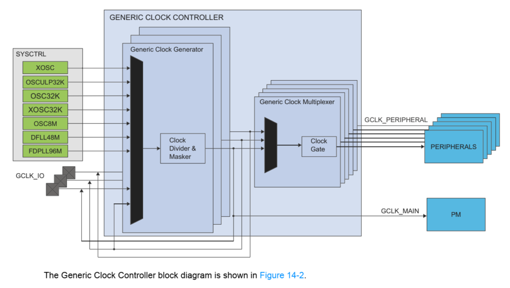
To configure a pin for PWM requires a good bit of effort. The basic idea is to select a clock source from SYSCTRL (such as the 48 MHz system clock) and connect it to a Generic Clock Generator. The SAMD21 has 9 different generators we can use. We can configure each generator to have its own divider and mask (so that we can run various peripherals off different speeds thanks to having separate clock generators).
Then, we connect our generator to the peripheral we want. In the example below, we’ll be using the Timer/Counter for Control Applications (TCC). The SAMD21 also has a Timer/Counter peripheral (TC), but from what I could grasp, it’s “TCC lite” (i.e. TCC with less features).
Once we have our peripheral configured (TCC, in this case), we then want to connect that to a hardware pin so that we get an actual waveform to appear.
While this might seem extremely complicated, the upside is that the SAMD21 is an extremely powerful chip. We can connect and configure different peripherals in many, many different ways (thanks to all this multiplexing of clock signals!).
Let’s walk through an example of outputting a 1 MHz square wave on pin PA18. Note that PA18 is D10 on the Arduino Zero, Adafruit Feather M0, and the SparkFun SAMD21 Mini Breakout board. If you don’t have one of these boards, check your schematic to see where PA18 goes. Also, note that there are lots of ways to output a 1 MHz square wave on a pin. We’ll be doing this using a 50% duty cycle PWM and the 48 MHz system clock.
Step 1: Enable Clock Source in SYSCTRL
You have a few options for clock sources:
- External oscillator (0.4 – 32 MHz)
- External oscillator at 32 kHz
- Internal oscillator at 32 kHz
- Ultra low power internal oscillator at 32 kHz
- Internal oscillator at 8 MHz
- Digital frequency-locked loop at 48 MHz
- Fractional digital phase-locked loop (48 – 96 MHz)
Some of these, like the phase-locked loop, can only be used to provide a clock signal for the peripherals. It cannot be used as a system clock. As such, the maximum processing speed of the SAMD21 is 48 MHz.
In most of the Arduino implementations of the SAMD21, the 48 MHz clock is already enabled for us (in the background, as part of the framework). That means we don’t need to initialize it our user code.
Step 2: Configure Clock Generator and Connect It to a Clock Source
Generic clock generators create a square wave (inside the chip) that we can frequency divide, mask, and connect to peripherals. The SAMD21 has 9 clock generators for us to use. We need to pick one, initialize it, and connect it to our clock source.
From what I could find, Generic Clock Generators 0 and 1 were used for other Arduino functions, so you probably want to avoid using those.
Step 3: Configure Peripheral and Connect It to a Clock Generator
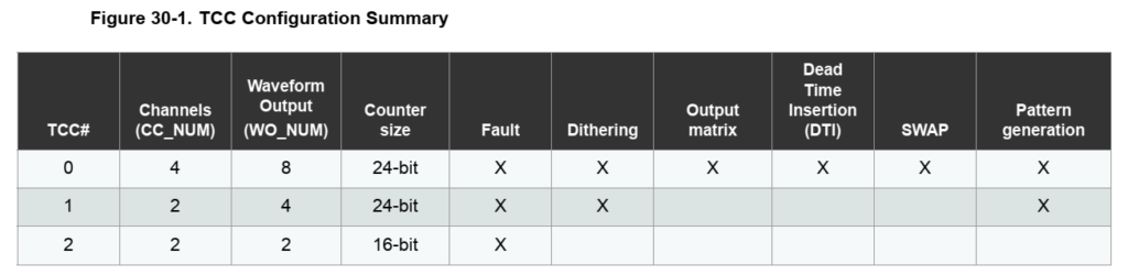
The SAMD21 has several peripherals for us to use. We’ll be focusing on the TCC for this example. There are 3 TCCs for us to use, and each one has its own set of unique features. TCC0 and 1 are 24 bits wide whereas TCC2 is limited to 16 bits for its counter. From section 30.1 (page 651) in the datasheet:
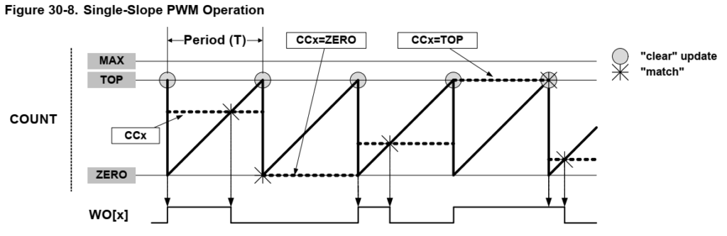
With TCC, we can set it to generate a PWM waveform on a pin. We will use a simple, single-slope PWM wave that counts up to a given value. During that counting process, if the value of the counter is equal to the Compare and Capture (CC) register, then the pin will toggle to low. Once the counter reaches the value in the Period (PER) register, then the pin will toggle back to high. The counter resets and starts over again.
From section 30.6.2.5 (page 660) in the datasheet, we get a diagram of how the PWM counter works. Note that TOP, for this mode, refers to the value in the PER register.
WO[x] stands for “waveform output,” and the x is the pin we wish to use. In the datasheet, navigate to section 6.1 (page 21) to see a chart of the pin to function mapping (too long to copy here). Under functions E and F, you’ll see the TCC options. For our PA18 example, you can see that function F is TCC0/WO[2].
Here is the really confusing part: there are only 4 CC options (CC0 through CC3) for setting the duty cycle, but the pin/function mapping chart shows up to WO[7] channels. So, how do we connect a given CC register to a WO pin that’s greater than 3? This poorly labeled chart buried away in part 30.6.3.7 (page 678) holds the key:
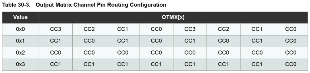
WO[7] is on the left and WO[0] is on the right. The OTMX configuration bits are found in the WEXCTRL register. By setting the OTMX bits to values 0-3, you can change which CC registers the various WO pins use.
By default, OTMX is set to 0x0, so the top row of the chart is used. Since we are using WO[2], we need to use CC2, according to the chart. If you want to use WO[5], you would use CC1.
Step 4: Set Data Direction and Peripheral for Pin
Because we’ve already configured TCC0/WO[2], that locks us in to pin PA18. Pins have a variety of functions that they can be set to (once again, refer to the chart in section 6.1). For our project, we need to set PA18 to Function F (TCC0/WO[2]). We also need to set PA18 as an output in the data direction (DIR) register.
Example Code
Now for the moment you’ve all been waiting for (or, let’s be honest, the part you scrolled down for, skipping the above descriptions). Here is some example Arduino code to create a 1 MHz square wave on PA18 (D10 on the Zero, Adafruit Feather M0, or SparkFun SAMD21 Mini).
Note: Many thanks to MartinL on the Arduino forums! Their code snippet (found here) helped me tremendously. The following code is based on that snippet.
// Number to count to with PWM (TOP value). Frequency can be calculated by
// freq = GCLK4_freq / (TCC0_prescaler * (1 + TOP_value))
// With TOP of 47, we get a 1 MHz square wave in this example
uint32_t period = 48 - 1;

void setup() {

  // Because we are using TCC0, limit period to 24 bits
  period = ( period < 0x00ffffff ) ? period : 0x00ffffff;

  // Enable and configure generic clock generator 4
  GCLK->GENCTRL.reg = GCLK_GENCTRL_IDC |          // Improve duty cycle
                      GCLK_GENCTRL_GENEN |        // Enable generic clock gen
                      GCLK_GENCTRL_SRC_DFLL48M |  // Select 48MHz as source
                      GCLK_GENCTRL_ID(4);         // Select GCLK4
  while (GCLK->STATUS.bit.SYNCBUSY);              // Wait for synchronization

  // Set clock divider of 1 to generic clock generator 4
  GCLK->GENDIV.reg = GCLK_GENDIV_DIV(1) |         // Divide 48 MHz by 1
                     GCLK_GENDIV_ID(4);           // Apply to GCLK4 4
  while (GCLK->STATUS.bit.SYNCBUSY);              // Wait for synchronization

  // Enable GCLK4 and connect it to TCC0 and TCC1
  GCLK->CLKCTRL.reg = GCLK_CLKCTRL_CLKEN |        // Enable generic clock
                      GCLK_CLKCTRL_GEN_GCLK4 |    // Select GCLK4
                      GCLK_CLKCTRL_ID_TCC0_TCC1;  // Feed GCLK4 to TCC0/1
  while (GCLK->STATUS.bit.SYNCBUSY);              // Wait for synchronization

  // Divide counter by 1 giving 48 MHz (20.83 ns) on each TCC0 tick
  TCC0->CTRLA.reg |= TCC_CTRLA_PRESCALER(TCC_CTRLA_PRESCALER_DIV1_Val);

  // Use "Normal PWM" (single-slope PWM): count up to PER, match on CC[n]
  TCC0->WAVE.reg = TCC_WAVE_WAVEGEN_NPWM;         // Select NPWM as waveform
  while (TCC0->SYNCBUSY.bit.WAVE);                // Wait for synchronization

  // Set the period (the number to count to (TOP) before resetting timer)
  TCC0->PER.reg = period;
  while (TCC0->SYNCBUSY.bit.PER);

  // Set PWM signal to output 50% duty cycle
  // n for CC[n] is determined by n = x % 4 where x is from WO[x]
  TCC0->CC[2].reg = period / 2;
  while (TCC0->SYNCBUSY.bit.CC2);

  // Configure PA18 (D10 on Arduino Zero) to be output
  PORT->Group[PORTA].DIRSET.reg = PORT_PA18;      // Set pin as output
  PORT->Group[PORTA].OUTCLR.reg = PORT_PA18;      // Set pin to low

  // Enable the port multiplexer for PA18
  PORT->Group[PORTA].PINCFG[18].reg |= PORT_PINCFG_PMUXEN;

  // Connect TCC0 timer to PA18. Function F is TCC0/WO[2] for PA18.
  // Odd pin num (2*n + 1): use PMUXO
  // Even pin num (2*n): use PMUXE
  PORT->Group[PORTA].PMUX[9].reg = PORT_PMUX_PMUXE_F;

  // Enable output (start PWM)
  TCC0->CTRLA.reg |= (TCC_CTRLA_ENABLE);
  while (TCC0->SYNCBUSY.bit.ENABLE);              // Wait for synchronization
}

void loop() {
  // Do nothing
}
Run it, and connect an oscilloscope to pin PA18. You should get a nice 1 MHz signal (well, as nice as you can expect from a microcontroller). Here is the output as measured on my Analog Discovery 2:
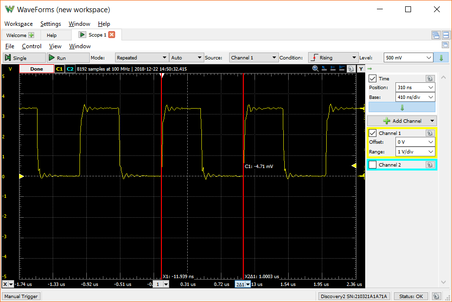
That’s it for the setup of a PWM timer on the SAMD21. Feel free to use the code as a starting point for your own project!
Next SAMD21 article: Arduino Zero (SAMD21) FDPLL with CMSIS
Edit [12/23/18]: Added section about TCC counter sizes and updated code to reflect unsigned 24 bit maximum for TCC0.
This has been very helpful; I am, unsure on a couple of items, if I want to change th TOP value (PER in this example) can I do it at any point? If I want to read or write the COUNT value is that possible and finally is it possible to generate an interrupt when the counter is reset after matching TOP? Many thanks
Yes, you should be able to update the TOP and COUNT registers at any time. You should also be able to generate an interrupt after COUNT reaches TOP. I have not touched a SAMD21 in a few years, so I don’t remember how to do those things. I recommend checking out this article to see how to generate interrupts with timers: https://microchipdeveloper.com/32arm:samd21-nvic-configuration
Thanks so much! I had overlooked that table 30-3 and was about to start scratching PCB traces to switch to an output that I could get to work.
Thank you for a very helpful tutorial.
I was using this outside of the arduino environment and was able to make it work changing only 2 things.
First was to select the 8MHz clock source instead of the 48MHz.
Second was to add the line “PM->APBCMASK.bit.TCC0_ = 1;” before setting up the timer.
I set the clock source to the 8MHz clock because it was already enabled.
I am guessing that the arduino code enables TCC0 in the power manager automatically, but I had to add the above line when using a more “raw” environment.
Thank You for a very clear and useful article! I succeeded finally in getting
my specific PWM needs met with the Arduino MKR WiFi 1010. It has the SAMD21
processor as well. Now I have two outputs producing two distinct PWM signals.
I can change the frequency and duty cycle for both separately and it all
works just the way I want it!
Your article was pleasant and easy enough to understand but the code example was not directly
applicable to the 1010 because the pin PA18 is not connected to an output of this
microcontroller board. When I changed the code so that it would give me an output on
some of the pins, it would not work. The solution came when I went to the
forum that you recommended and finally found it: The code lines in your example
toward the end:
// Connect TCC0 timer to PA18. Function F is TCC0/WO[2] for PA18.
// Odd pin num (2*n + 1): use PMUXO
// Even pin num (2*n): use PMUXE
PORT->Group[PORTA].PMUX[9].reg = PORT_PMUX_PMUXE_F;
has that PMUX[9] hardcoded niner. This works fine on port PA19 and PA18 but not
on others. It appears it would work if I replace the
9 with my port number shifted by 2, for PA??: ..PMUX[?? >> 1]..
PORT->Group[PORTA].PMUX[?? >> 1].reg = PORT_PMUX_PMUXE_F;
This would then work well for many of the ports.
I came upon this site while looking for a solution to a problem with the SAMD21 TCC that shouldn’t exist, according to the docs.
The problem is I want to dynamically change both the frequency and the duty of the PWM. Reading the specs, this should be achievable using the double buffering feature, And it works very nicely, for the duty (the CC register), the width increases or decreases smoothly, there are no glitches. But do what I may, I can’t make it work for the TOP register. LUPD bit on or off, no matter, it behaves as if written directly. When the frequency decreases, this is fine, since the TOP has a bigger value and is reached. But when the frequency increases, the value is smaller and the counter wraps around before triggering. I was finally able to make it work by forcing a retrigger (control B CMD = 01) after writing the new TOP, but of course there appears a broken pulse in the sequence this way. I probably could fix that too by attaching an interrupt to the event of counter wraparound, and writing the next TOP then, but this is overkill and shouldn’t be needed if the double buffering feature was working as advertised.
So the question is – have you seen this problem or maybe an explanation/solution?
In your code you write:
// Configure PA18 (D10 on Arduino Zero) to be output
PORT->Group[PORTA].DIRSET.reg = PORT_PA18; // Set pin as output
PORT->Group[PORTA].OUTCLR.reg = PORT_PA18; // Set pin to low
PORTA is defined as:
#define PORT_PA18 (_UL_(1) <Group[PIN_PA18 / 32].DIRSET.reg = PORTA;