Placing Parts in the Schematic
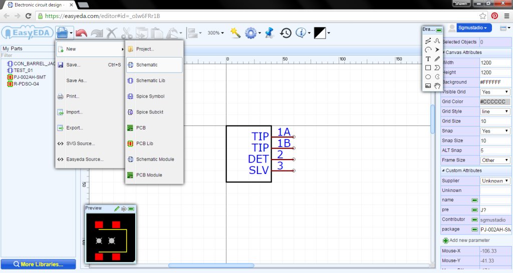
We made the parts we need in Part 1, so now we can create the schematic for our linear regulator. Click on the File icon, select New, and click Schematic.
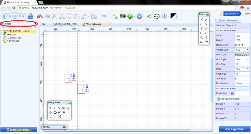
In the parts selector, make sure My Parts is selected, click on our custom part (CON_BARREL_JACK), and click somewhere on the schematic to place the part.
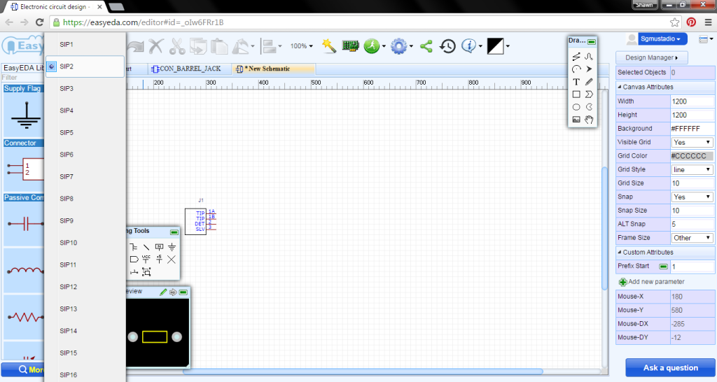
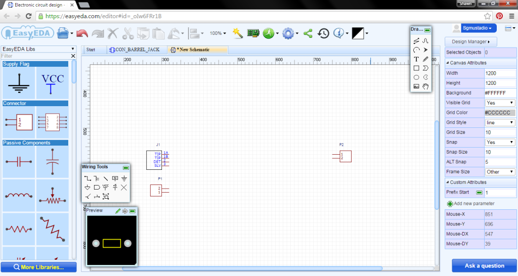
Next, let’s add some basic 2-pin headers. Change the parts selector to EasyEDA Libs, select the drop-down menu under the one-sided connector, and click SIP2.
Place 2 of these–one on each side of the schematic. Press the r key to rotate the part while on the cursor. We will want these to plug into our breadboard.
Next, we want to add a couple of surface mount diodes. EasyEDA does not have the diode footprint we want, but luckily, we can add it from a user-generated part.
Importing Other Users’ Footprints
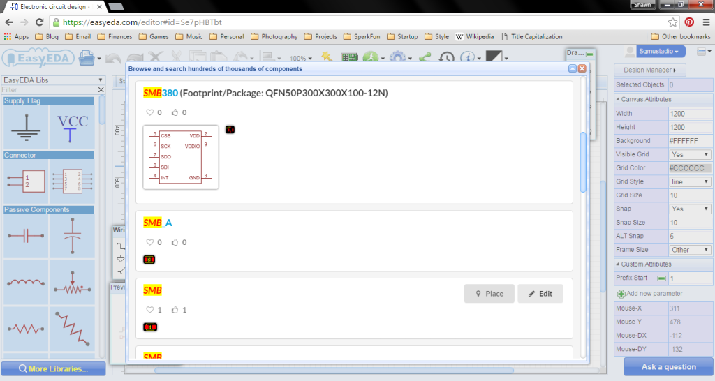
From the parts selector, click on EasyEDA Libs. At the bottom of that pane, click More Libraries… A new search box will appear. Type in SMB and hit enter.
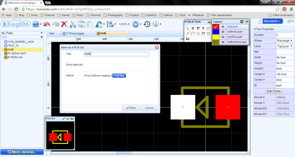
Scroll down and click Edit on the first SMB package. This will open up the package editor again. You can check the dimensions of the footprint. They’re slightly off from what the datasheet asks for, but it’ll do.
We also need to change the name of one of the pads. Click on the K pad, and change its name to C. This will matter when we pair it with the schematic part. Click the file icon and Save As.
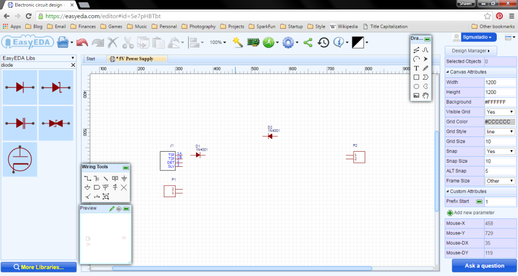
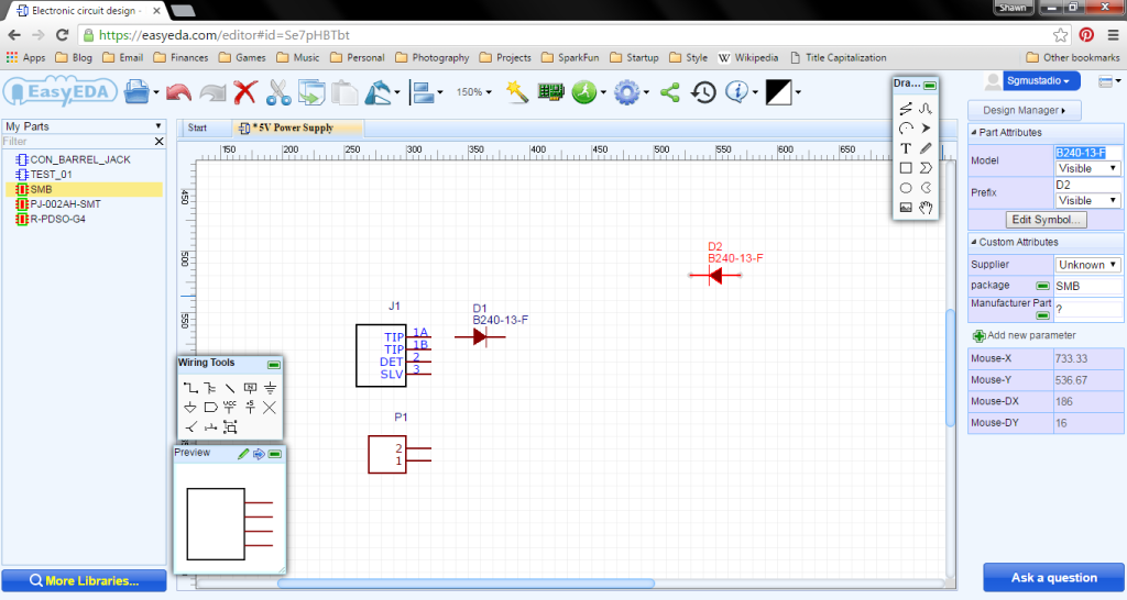
Click Save, and close out of the package editor tab (so you are back in the schematic editor). In the part selector pane, search for diode. Click on the first symbol (regular diode) and place two of them in the schematic. Note the polarity of the second diode!
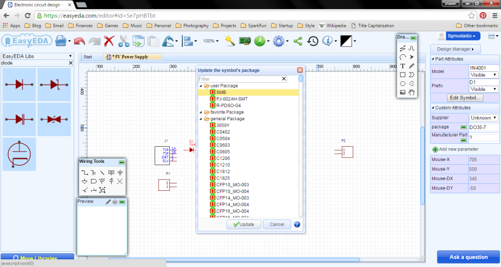
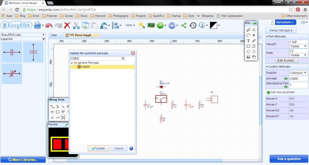
Press esc to stop placing parts, and click on the first diode. In the Custom Attributes section of the right-side pane, click on the package property to bring up the package selector box. Under User Package, select SMB, and click Update.
Repeat this process for the second diode. Now, both diodes will have the SMB package.
For both diodes, change the Model to B240-13-F to match the part from Digi-Key. This can be found in the Part Attributes section of the right-side pane.
Adding the Rest of the Components
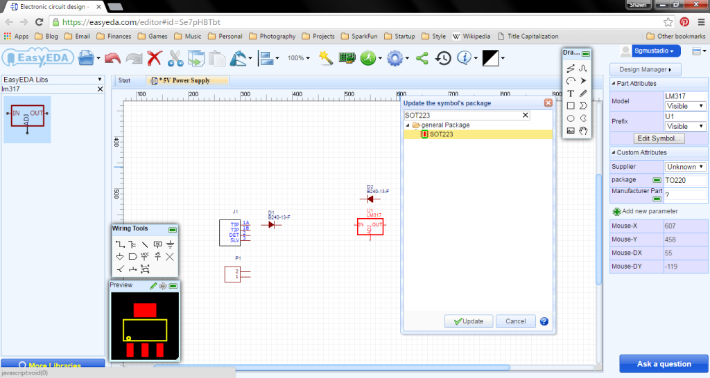
Use the part selector pane (left side) to search for LM317 (our voltage regulator), place it below the second diode, and change its package to a SOT223 (surface mount).
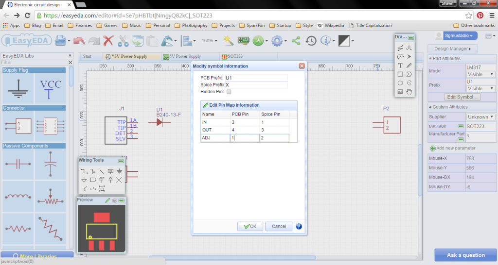
Unfortunately, the pins on the schematic part do not match correctly with the pins on the footprint (according to the datasheet). With the LM317 selected, click on Edit Symbol… (button under Part Attributes in the right-side pane) and change the pins under PCB Pin:
- IN: 3
- OUT: 4
- ADJ: 1
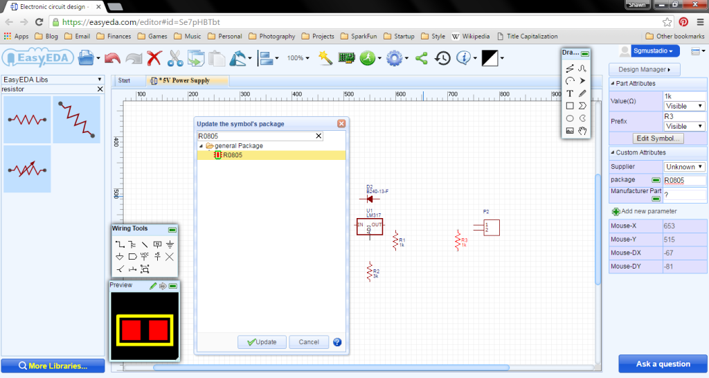
Click OK. Search for a place 3 resistors. Change the value of the one directly under the LM317 to 3k, and leave the others at 1k. Change all of the packages to R0805.
Place two capacitors around the LM317 and change their packages to C0805. For the capacitor to the left of the LM317, change its value to 0.1uF, and change the other’s value to 1.0uF.
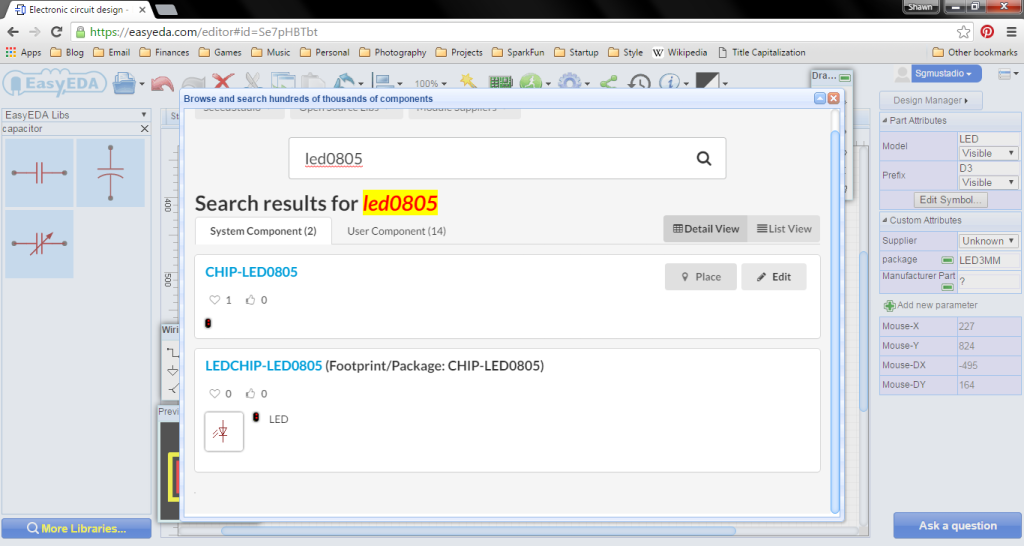
We need to add a chip footprint for our LED before we place the schematic part. In More Libraries…, search for and edit LED_0805.
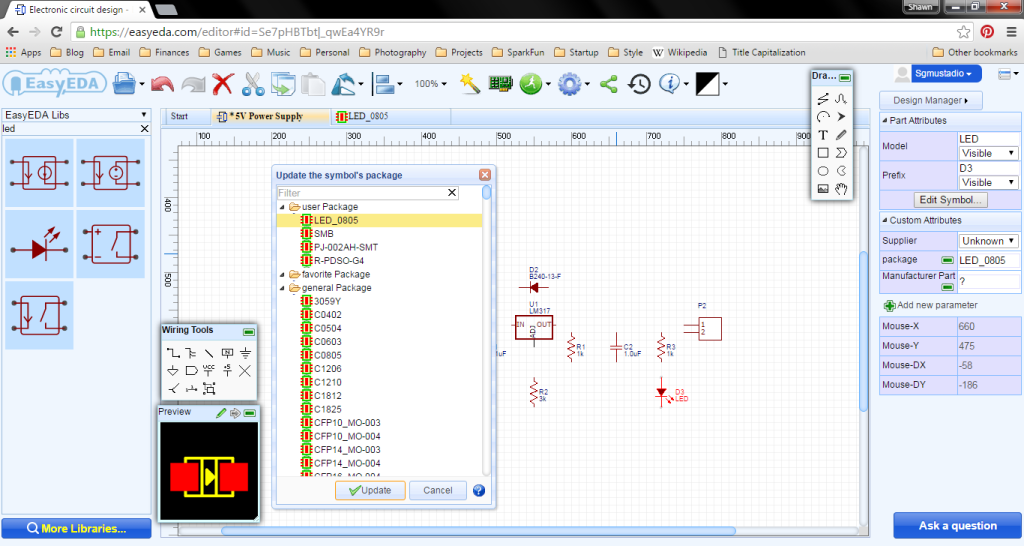
Save as on the new part to save it in your library. Find the schematic part LED, place it below the third resistor, and change its package to LED_0805.
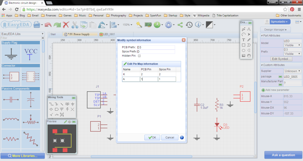
Unfortunately, the pins on the schematic part and PCB footprint do not match up for the LED we just placed. Under Part Attributes, click Edit Symbol… Change the PCB pins to 2 and 1 (to match up with K and A, respectively).
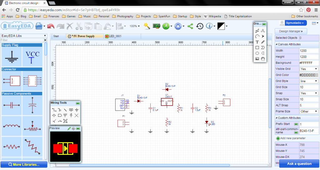
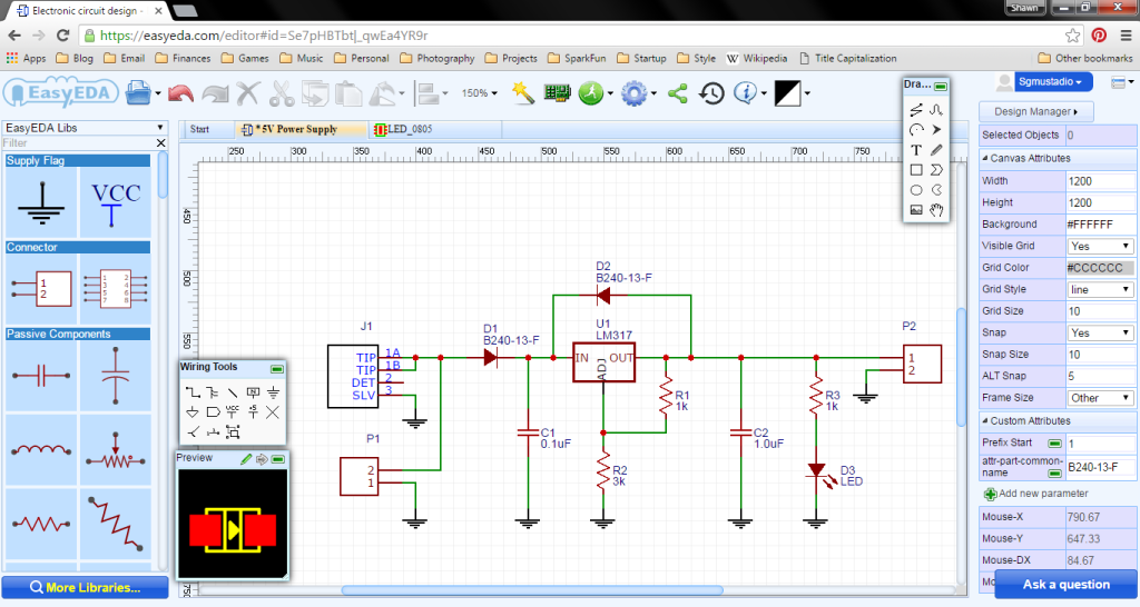
Click OK. Under EasyEDA Libs, add Ground supply flags under all the nodes that will be connected to ground. Feel free to drag some of the components to move them closer to each other.
Connecting Wires
Using Wire in the Wiring Tools box, make connections to all our components.
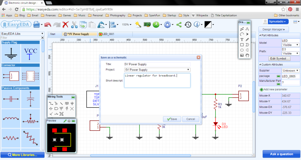
Click File > Save As. Give the schematic an appropriate name (e.g. “5V Power Supply”), and select 5V Power Supply under Project.
Click Save.
Generate Bill of Materials
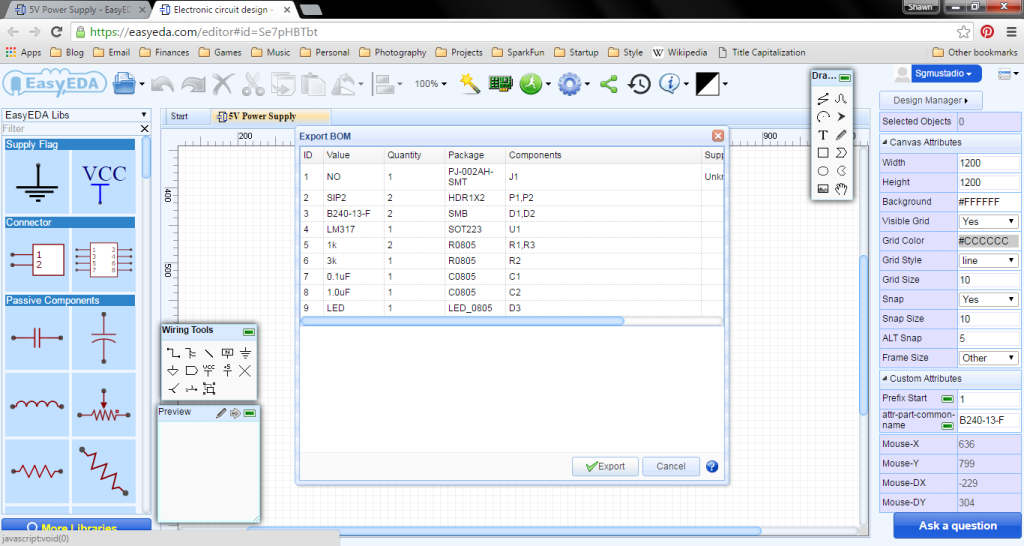
Before moving on to layout, we want to generate our bill of materials (BOM). This will tell us what to order and where to solder parts when the PCB is made.
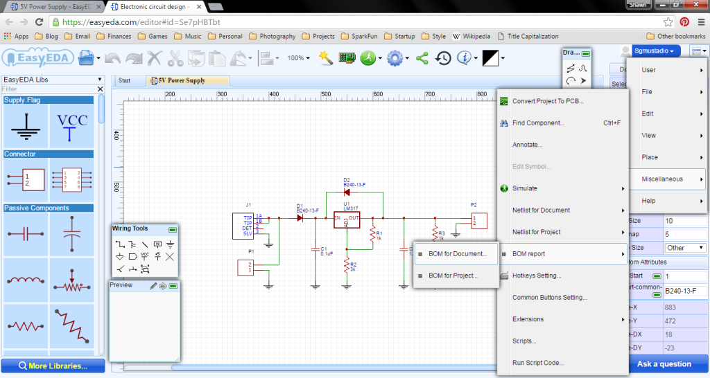
Click the Menu button at the top-right of the window, select Miscellaneous > BOM Report > BOM for Document.
A new window opens up and lets us export the BOM as a comma-separated value (CSV) sheet.
Click Export. If you would like to make this board, I’ve added links to the Digi-Key parts to the BOM: 5V_Power_Supply_BOM
Schematic capture is done! Tomorrow, we’ll layout the PCB.

One thought on “Getting Started with EasyEDA Part 2: Schematic Capture”